Electronic devices permeate our everyday lives and have an impact on everything we do. Their prevalence represents the great success of the silicon age. Silicon is a common material in many of the ubiquitous electronic devices that we engage with and rely on today. Yet, a pressing question for scientists today is what material will define the age of tomorrow?
An exciting class of materials known as two-dimensional (2D) materials might be the answer. By implementing these materials into devices, their unusual quantum properties such as confinement, electron-electron correlations, superconductivity, and topology can be harnessed and exploited to yield devices with new modalities, high performance, and low power consumption.
The Velasco lab is an experimental materials/condensed matter group that specialize in the fabrication and characterization of novel 2D material devices with unprecedented sensitivity and atomic scale precision. Our aim is to attain a deep and fundamental understanding of the electronic properties of 2D material devices.
Below our major research thrusts are outlined. Our characterization schemes are closely related, as they resolve the real-space and momentum-space electronic structures of 2D material devices. Together these techniques deliver a comprehensive picture of the electronic structure unattainable with the use of solely one experimental technique.
1. Scanning Tunneling Microscopy/Spectroscopy(STM/STS)
In this thrust we use the STM to visualize and manipulate the electron waves residing on the surfaces of 2D quantum materials. This enables further fundamental insight on the electronic properties of 2D quantum materials. Example projects include trapping and imaging Dirac electrons hosted by graphene and bilayer graphene, and direct low energy band structure visualization.
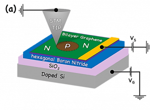
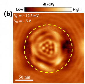
Figure 1: STM/STS of 2D quantum material devices. (a) Schematic of a STM tip probing a circular p−n junction in Bernal stacked bilayer graphene (BLG) that is supported by hexagonal boron nitride (hBN). The BLG/hBN heterostructure rests on a SiO2/doped Si wafer. The STM tip is grounded, a sample bias(Vs) is applied between the BLG and ground, and a gate voltage (VG) is applied between the doped Si and BLG. (b) Constant sample bias dI/dVS maps of circular BLG p−n junctions. The yellow dashed line in (b) denotes the boundary between p and n doped regions.
Related publications: (1) Z. Ge et al., Nano Letters 2020; (2) Z. Ge et al., Phys. Rev. Lett. 2021; (3) Z. Ge et al., Nano Letters 2021; (4) F. Joucken et al., Nano Letters 2021; (5) F. Joucken et al., Phys. Rev. Lett. 2021
2. Nanospot Angle Resolved Photoemission Spectroscopy (ARPES)
In this thrust we use an ARPES microscope with sub micron resolution to directly visualize and spatially map the electronic band structure of 2D quantum material devices. This enables visualization of topological transitions and many-body spectral reconstructions that are induced and manipulated by electric fields. Such visualization could validate untested theories regarding many-body interactions and new topological properties and transform our understanding of electronic devices based on 2D materials.
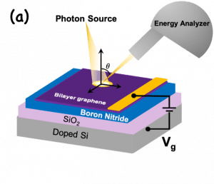
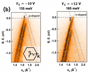
Figure 2: NanoARPES of 2D quantum material devices. (a) A photon source shines on the BLG/hBN heterostructure device surface and reflected light is collected by an energy analyzer. This scheme can directly probe the BLG band structure, band structure modifications due interactions between BLG and hBN, and band structures at different Fermi levels. (b) ARPES E-k spectra obtained at gate voltages of -10 V (p-doped) and +12V (n-doped). Left axis is the binding energy (B. E.); bottom axis is the in-plane momentum. The Fermi level (B. E.=0 eV) is denoted by a dashed black line in each spectrum. The tight-binding bands are superimposed on each spectrum. Inset of left panel in (b) indicates the direction of the measurement.
Related publications: (1) F. Joucken Nano Letters 2019; (2) F. Joucken Phys. Rev. B (Rapid) 2019
3. Tunneling Spectroscopy via planar tunnel junctions
In this thrust we use a planar tunnel junction composed of 2D materials to measure the single particle density of states (SPDOS) of 2D quantum materials at ultra low temperatures(~250mK) and exceptionally high magnetic fields (18T). The SPDOS is directly calculable and encodes the nature of electron-electron interactions, which are abundant in extreme experimental conditions such as millikelvin temperatures and ultra-high magnetic fields.
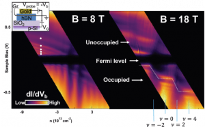
Figure 3: Planar tunneling spectroscopy in ultra high magnetic fields and low temperatures. Tunneling spectroscopy maps of graphene at B = 8 T and B = 18 T. At 18T several Landau levels(LLs) are visible including LLs due to broken symmetry states such as ν=0 and ν=4.
Related publication: J. Davenport Appl. Phys. Lett. 2019
Interested prospective PhD students should apply to the physics department at UCSC. Funding opportunities exist in the form of research and teaching assistantships.
For more information please contact Professor Velasco at jvelasc5@ucsc.edu.